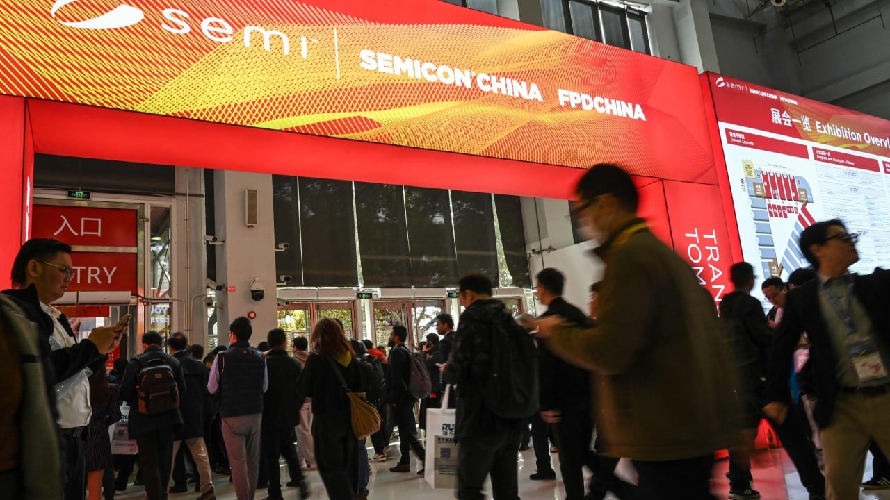
The floor of the Shanghai New International Expo Centre is humming with a tension that has nothing to do with the heavy machinery on display. At Semicon China 2026, the 1,500 exhibitors are not just selling tools; they are pitching a survival strategy. For years, the global semiconductor narrative focused on the "choke point"—the idea that denying China access to 5nm or 3nm lithography would effectively freeze its technological progress. That theory has hit a hard reality. Instead of waiting for a breakthrough in forbidden EUV (Extreme Ultraviolet) scanners, China has pivoted its entire industrial apparatus toward advanced packaging and heterogeneous integration.
This shift is the primary driver of the country's projected chip industry growth in 2026. By stacking older, less-sophisticated chips (the "chiplet" approach) and linking them with ultra-fast interconnects, domestic firms are producing AI accelerators that rival the performance of restricted Western silicon. It is a brute-force architectural solution to a manufacturing constraint.
The Chiplet Workaround
Western export controls effectively banned the sale of the highest-end GPUs, such as NVIDIA’s Blackwell series, to Chinese entities. However, the 2026 showcase reveals that firms like Huawei and Biren Technology have found the gap in the fence. They are utilizing 2.5D and 3D packaging to combine multiple 14nm or 7nm dies into a single high-performance package.
This technique, often called "Heterogeneous Integration," allows a company to take three or four functional blocks—compute, memory, and I/O—and stitch them together on a silicon interposer. The result is a chip that, for specific AI training tasks, performs at a level the U.S. Department of Commerce intended to block. It is less power-efficient than a monolithic 3nm chip, but in a world of sanctions, efficiency is a luxury; availability is the only metric that matters.
The High Bandwidth Memory Breakthrough
If the compute die is the brain of AI, High Bandwidth Memory (HBM) is the nervous system. Without it, the fastest processor in the world sits idle, waiting for data. For the past two years, the industry watched closely to see if China could replicate the complex stacking required for HBM3 and HBM4.
The 2026 data confirms a significant milestone. Local memory champion CXMT (ChangXin Memory Technologies), in coordination with Huawei, has moved into mass production of domestic HBM solutions, specifically the HiBL 1.0 and HiZQ 2.0. While these may still trail the absolute peak bandwidth of SK Hynix’s latest 16-high stacks, they are sufficient to power the Ascend 950PR, Huawei’s 2026 flagship AI processor.
The speed of this development has caught many analysts off guard. It suggests that the "rocket fuel" provided by U.S. controls—as one industry veteran described it—has forced a level of state-directed R&D coordination that would have taken a decade in a free-market environment.
Geopolitical Friction and the Trump Recalibration
The backdrop to this technical surge is a confusing shift in Washington. As of early 2026, the Trump administration has signaled a more transactional approach to chip exports. The December 2025 decision to approve licenses for certain mid-tier AI chips, like NVIDIA’s H200 (in a modified "China-specific" form), was intended to preserve U.S. market share and prevent a total decoupling that would bankrupt American toolmakers.
However, the "AI OVERWATCH Act" currently moving through the U.S. House of Representatives threatens to claw back that licensing authority. This creates a volatile environment for Chinese tech giants. They cannot trust the supply of Western chips, even when licenses are granted. Consequently, the "Buy Domestic" mandate from Beijing has evolved from a patriotic suggestion to a hard requirement for any company receiving state subsidies.
Domestic Toolmakers Gain Ground
The most telling metric of 2026 is not found in the chips themselves, but in the machines that make them. At previous Semicon China events, domestic equipment was often tucked away in smaller booths, viewed as "good enough" for legacy nodes but irrelevant for the cutting edge.
That has changed.
- Etch and Deposition: Domestic leaders like AMEC and Naura are now supplying nearly 50% of the tools for new domestic fabs.
- Advanced Packaging Equipment: Because packaging is not yet as heavily restricted as front-end lithography, China has been able to import sophisticated "back-end" tools from Japan and Europe, which they are now reverse-engineering and improving upon.
- The Yield Factor: The industry’s dirty secret is that while China can make 7nm chips, the "yield"—the percentage of working chips per wafer—remains low. Advanced packaging helps mitigate this. By using smaller "chiplets," the probability of a defect ruining the entire package is lower than it would be on a massive, single-die chip.
The Power Constraint
For all the progress in silicon, a different bottleneck has emerged: electricity. The surge in domestic AI data centers is straining China’s regional grids. At Semicon China 2026, a new focus has emerged on Power Management ICs (PMICs) and Silicon Carbide (SiC).
As AI models grow, the power required to move data between the processor and memory creates heat levels that traditional cooling cannot handle. This is driving a secondary boom in liquid cooling and specialized power delivery chips. China is currently the world leader in SiC production, largely due to its massive electric vehicle (EV) market. This expertise is being cross-pollinated into the server room, creating a uniquely Chinese ecosystem where the EV supply chain is subsidizing the AI infrastructure.
A Divergent Future
We are witnessing the birth of two distinct semiconductor universes. One is led by the U.S., focusing on monolithic scaling and pushing the physical limits of 2nm and beyond using ASML’s most advanced High-NA EUV machines. The other is led by China, focusing on architectural ingenuity, massive-scale packaging, and a "good enough" approach to lithography that prioritizes volume and sovereignty over absolute power efficiency.
The "choke point" strategy has not stopped China; it has merely changed the shape of its growth. The 2026 industry peak, with global sales nearing $1 trillion, is being fueled by an AI boom that no single government can fully contain. For the veteran analyst, the lesson is clear: you can restrict a specific tool, but you cannot restrict the laws of physics or the desperation of a superpower with unlimited capital.
The focus now moves to the next frontier: optical interconnects and silicon photonics. If China can master the art of moving data with light instead of electricity at the package level, the lithography gap may become a historical footnote.